Activity
Mon
Wed
Fri
Sun
Mar
Apr
May
Jun
Jul
Aug
Sep
Oct
Nov
Dec
Jan
Feb
What is this?
Less
More
Memberships
LeadIn Sales & Influence Club
21 members • Free
Fresuelectronics.com
1.6k members • Free
2 contributions to Fresuelectronics.com

Jul '24 •
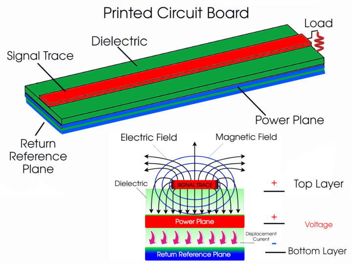
Be aware of using Power Planes as Return Reference Planes!
Back when I started designing PCBs I heard it was pretty common to use power planes as Return Reference Planes (RRP), and I still see that this is widely used in the industry. An example is the "classic" 4-layer stackup: - SIGNAL - POWER - "GROUND" - SIGNAL One of the problems we have with this stackup is that the signal on the top layer uses the power plane as a path for the current to close the loop and return to the source. But how does it actually close the loop if the POWER plane is DC disconnected from the "GROUND" plane? Unfortunately, it does so through the displacement current, which has to cross the impedance between the POWER plane and the "GROUND" plane. This means that when this happens, the current flowing through the impedance between the planes will generate a voltage drop, which will impact the whole board and eventually affect EMI. And yes, I know the common recommendation is to add decoupling capacitors, but unfortunately, this will only work up to certain frequencies due to the impedance profile of the capacitor. The best scenario is to have the Return Reference Plane adjacent to the signal layer. However, if we are forced to use the power plane option, make sure that the impedance between the POWER plane and the "GROUND" plane is as small as possible so that the voltage drop is minimized. One way to achieve this is to reduce the distance between the planes as much as possible, which will increase the interplane capacitance and lower its impedance. I hope this helps, Dario

1 like • Jul '24
I wonder, if the assumption you made, is correct in all circumstances. I think it was Eric Bogatin, who mentioned in one video, that you can use a power plane as the reference plane, if it has a low impedance connection to the driver of the signal. That make sense to me, since the lowest impedance path for the displacement current would be right through the driver's power pins then. Intuitively I would expect, that you could get a little more noise on that power rail, but the current loop would still be well defined. When the referenced power plane does not meet this requirement, you are absolutely right. The displacement currents can go anywhere. From the overall design perspective, I would only use that as a last resort though, since you have even more things to watch out for (split planes, coupling to adjacent planes etc.).
Jul '24 •
Want to Pass EMC tests? Avoid this...
What classical circuit theory fails to teach you about designing Printed Circuit Boards (PCBs) is that it’s not about electrons moving through traces like water through pipes. This is why not many PCB designs pass EMC tests on the first attempt, because many are designed with this incorrect concept in mind. The circuit you see here has only two layers, both dedicated to signal traces. Here is why the chances of passing EMC are extremely low: - No consideration of how electromagnetic fields spread from the conductor traces. - No consideration of how current loops are directly related to radiated emissions. - No consideration of how common mode voltage drives antenna patterns once the cables are connected. - No consideration of how signals do not see a characteristic impedance along their propagation, leading to signal integrity failures. - No consideration of the impedance discontinuities signals encounter when crossing splits and other traces. - No consideration of crosstalk and its impact on emissions and board performance. - No considerations about return current and reference voltage during signal propagation. The list goes on and on... The same applies to immunity to external interferences, of course. I mention this because I want to help you understand that these are the common failures when your board does not pass EMC tests. 95% of EMI issues can be addressed at the layout stage. This means you can design the PCB correctly from the start. You don't need to have four iterations of your board to finally pass the test. EMC is all about prevention, not last-minute ferrite beads and copper tape SOS techniques. I hope this helps you see that there are ways to take your designs to the next level. But for that, you have to think in terms of Electromagnetic fields. Dario P.S. If EMI is still an issue, we can help. You can join us here: EMC Design Academy

4 likes • Jul '24
Let me just give you my 2cents on what you laid out so far: Regarding the 2-layer-board: Probably not the best decision to go for only 2 layers. 1. You are using switching regulators, that usually create high frequency ripple currents that in turn cause EM radiation if not confined in a proper way. Always think of where current flows and try to minimize the area of that current loop. Furthermore make sure that fast switching signals see a constant impedance, which usually means having a reference (ground)-plane next to the signal layer. 2. I would go for at least 4 layers with a solid ground plane underneath the regulators. That helps to confine the EM-fields to a small area and provides a proper return path for the signals. The ground plane will also help to distribute the heat away from the regulators, especially when you can connect it with lots of vias to the large ground pad (which the regulator probably have). If you absolutely have to stick to 2 layers, you could try define shield rings around the noisy nodes. But that will be much less effective than a continuous reference plane. Heat distribution is also more difficult if you only have two layers. It could work if you can do the routing (mostly) on one layer and use the other layer as a ground plane. Additionally you could use 70µm copper layers to increase thermal conductivity but I would rather go for 4 layers due to the EMC benefits. 3. For the 6-layer board it should not be difficult to keep temperature in check. Again, connect the ground pads of the heat producing components to the ground planes. 4. Regarding EMC I would make the stackup symmetrical, with the 5th layer being a ground plane. You want to confine the EM-fields of your signals. So always keep in mind, what your signals couple with via capacitive and inductive coupling. Try to avoid coupling to other signals and split planes since that will increase the risk of EMC problems. 5. If would distribute power on layer 3 and/or 4. Ask yourself if you really need ground planes. Often you easily get away with routed power. Then you can probably make layer 3 or 4 a solid ground plane too which further benefits your EMC performance. As far as I can remember I never really needed more the 3 signal/power layers when no BGAs were involved. It is all a question of proper component placement. 6. Watch videos with e.g. Eric Bogatin and Rick Hartley. These will help you a lot to understand the core principles.
1-2 of 2

@matthias-hafner-1375
Electrical engineer with 20 years experience in PCB design, embedded control systems etc.
Dr. degree in optical engineering.
Active 2d ago
Joined Jul 18, 2024