Activity
Mon
Wed
Fri
Sun
Jan
Feb
Mar
Apr
May
Jun
Jul
Aug
Sep
Oct
Nov
Dec
What is this?
Less
More
Memberships
The No Code AI Agency Startup
2.4k members • Free
Upscale (Free)
24.9k members • Free
Fresuelectronics.com
1.6k members • Free
Performance Marketer Academy
1.2k members • Free
2 contributions to Fresuelectronics.com

Aug '24 •
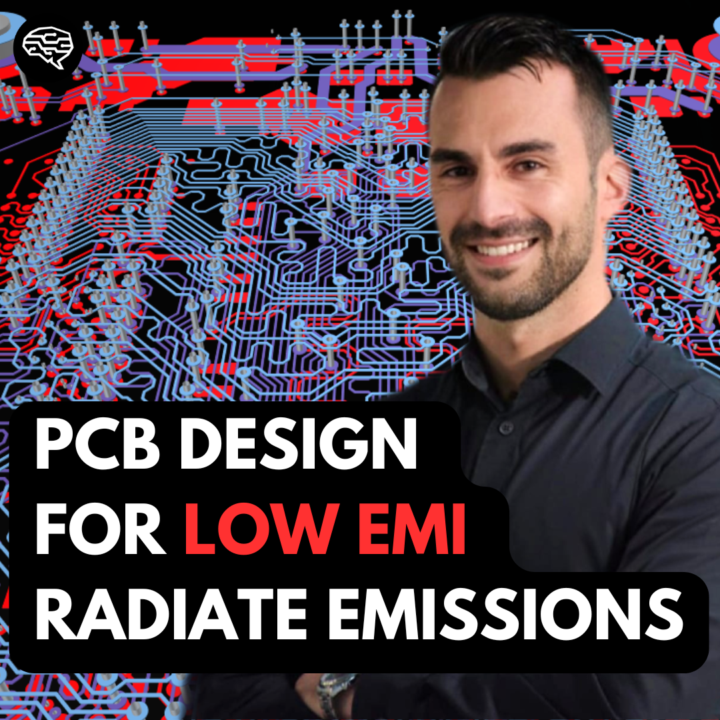
PCB Design for Low EMI: How to Minimize Radiated Emissions.
I just released my latest video, over 40 minutes long, where I dive deep into Radiated Emissions. I discuss how they are generated, how they depend on PCB design layout, and what we can do to minimize these effects. Watch the video for free here: youtu.be/Yg3QYT9wFqM Don't forget to leave a like if you enjoyed the video. This will help me create more content so we can stop the "EMI is Black Magic" nonsense. Enjoy! Dario --------------------------------------- PS: If you're struggling and need 1-on-1 support with fixing EMI issues on your PCB, DM me "HELP" and I'll personally get back to you.

2 likes • Aug '24
Thanks @Dario Fresu , very well explained with didactical diagrams and equations to keep simple as possible, but deep in knowledge.
Jul '24 •
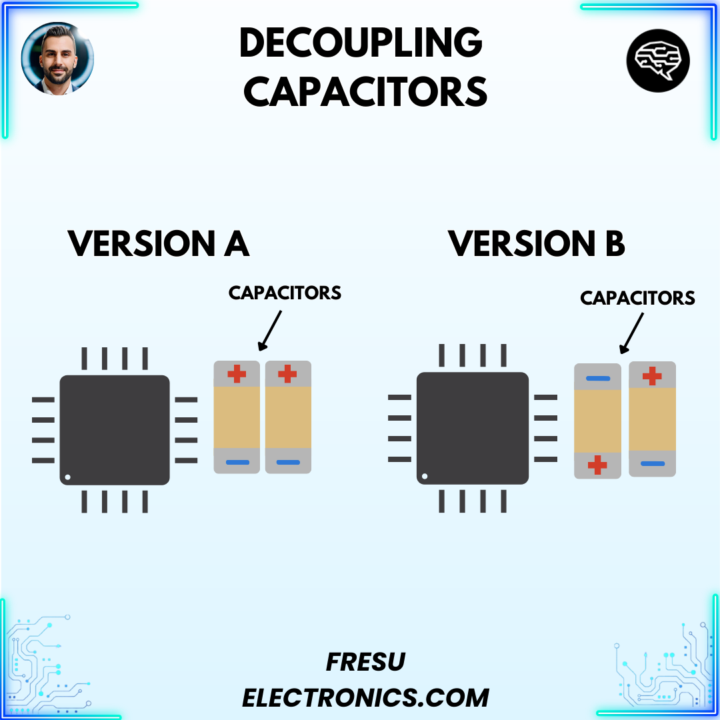
Decoupling Capacitor Strategies
Which version would give you the most effective decoupling strategy? Certain PCB designs require you to be extremely careful with your choices to improve your Power Delivery Network (PDN). If this were the case, what would you choose, and why?
Poll
82 members have voted
4 likes • Jul '24
@Dario Fresu thanks for this resource. Mutual inductance of vias is a new concept for me, thinking these are short length due the stack. Unfortunatelly some pictures on the document are corrupted.
1-2 of 2

@jose-pedraza-8363
Electronic Engineer with experience in PCB design using tools like Altium, Eagle, Cadence, Kicad.
Active 7d ago
Joined Jul 13, 2024
Colombia