Activity
Mon
Wed
Fri
Sun
Apr
May
Jun
Jul
Aug
Sep
Oct
Nov
Dec
Jan
Feb
Mar
What is this?
Less
More
Memberships
Fresuelectronics.com
1.6k members • Free
1 contribution to Fresuelectronics.com

Aug '24 •
ESC design course
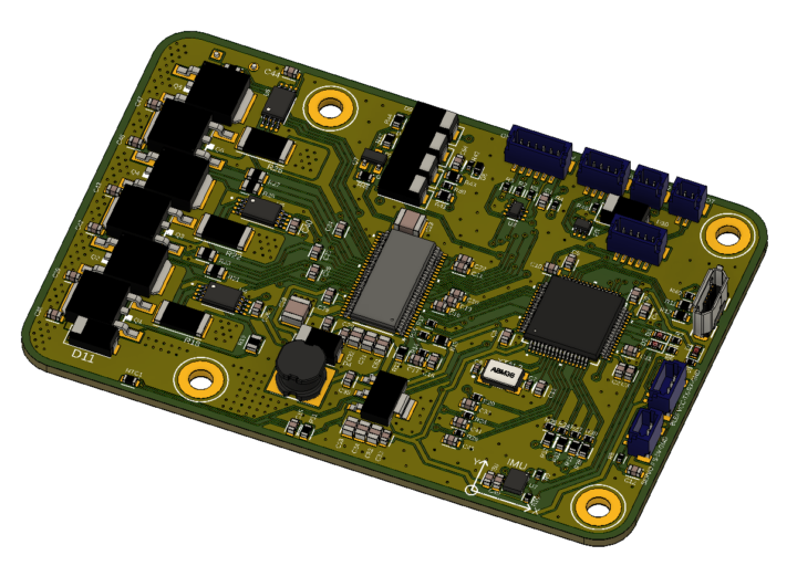
Hello everyone, ⚠️ Peer Review Request ⚠️ I have been learning electronics on the side and have discovered incredible value in following the courses here. Thanks a lot, Dario, for the amazing quality of the content. The structure of the course is extremely well done. Before taking the course, I wasn't certain how to approach this kind of design, but I now feel that the steps you provide create a very solid method. I am happy to present the first version of my ESC, slightly modified and inspired by Dario's version, as well as the VESC 6.5 and 6.4 schematic (from Benjamin Vedder's page). The main differences in this version are the following: - Based on VESC 6 (and not VESC 4) - E-switch integration (using the EN_BUCK pin of the DRV) with auto ON-OFF - Features an IMU onboard - BMI160 - Uses JST SH connectors - Scaled-down power stage - designed for 25A continuous current - Board size: 83 mm x 55 mm - The board is stacked as recommended in the course: Signal - GND - GND - Signal with 1 oz copper. - Designed with Fusion 360 electronic (Sorry KiCad, I was in Eagle first). I would love to receive feedback on the e-switch section, the layout in general (as this is my first attempt at making this kind of board), and any other relevant points you see in order to make this project a success. Once everything looks good, I will place an order with JLCPCB 🙌 Thank you all for the help 😁

2 likes • Aug '24
Hi Alexis, looks good! although the big BJT/FETs on the left side seem a bit too close to each other for manufacturing purposes, pick and place machines that place smd components usually need a bit of space around each component. this is the same for smaller SMD components.
1 like • Aug '24
@Alexis Plabat yes there are, usually Kicad and other EDA's(tooling) provide a Keepout/Clearance area. that area specifies the minimum bordering around a component for placement etc. But usually it's a good habit to check the datasheet of those components, manufacturers often provide their own minimum requirements down at the datasheet under the fabrication section. :) happy designing.
1-1 of 1

@jeffrey-dijkstra-8545
Just graduated Embedded electronics engineer that likes to build and design IOT pcb’s.
Active 11d ago
Joined Jul 31, 2024