Activity
Mon
Wed
Fri
Sun
Aug
Sep
Oct
Nov
Dec
Jan
Feb
Mar
Apr
May
Jun
What is this?
Less
More
Memberships
Fresuelectronics.com
1.6k members • Free
1 contribution to Fresuelectronics.com

Sep '25 •
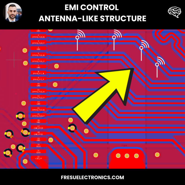
It doesn’t take much for a PCB to fail an EMC test.
One of the most common issues we encounter during reviews is the presence of antenna-like structures. These are often overlooked but can have a huge impact on electromagnetic behavior. A frequent source of this problem comes from copper pours. Designers usually don’t see them as risky, especially when they’re tied to nets like GND or power rails. The assumption is that any coupled signals will be safely absorbed and neutralized. In practice, however, the results are very different. These copper areas can behave like slot antennas, radiating unwanted energy. On top of that, they disturb the impedance of signals during propagation. This misunderstanding often comes from thinking of signals as electrons flowing through copper, moving from source to sink. While this model is widespread, it hides the real picture. In reality, signals travel as electromagnetic fields in the dielectric space around the conductors. With this perspective, it becomes clear that any nearby conductor, not properly engineered, can interfere and create problems. This concept is rarely explained in school and is often discovered only after costly trial and error, when EMC tests reveal that things don’t work as intended. At that point, we realize we need better, more intuitive models to truly understand what’s happening. So, keep an eye out for these seemingly harmless structures. They can jeopardize your entire project and budget by causing EMC test failures. To electromagnetic enlightenment, Dario P.S. If you’re still unsure how to put these concepts into practice and want to master EMI control, join my EMC/EMI Design Course Here

0 likes • Sep '25
What is the best way to fix the error shown in the example image? Should the antenna-like copper structure be removed, or should be it connected more effectively to the GND plane with redundant vias/traces to avoid it behaving it behaving like an antenna?
1-1 of 1

@andres-molina-3287
Electronics engineer with a master's degree in biomedical engineering. At present, I'm working on developing PCBs for medical equipment.
Active 19d ago
Joined Sep 25, 2025